Tag: ai-chips

  • Samsung Electronics Nears $146.6 Billion Cash Pile on AI Chip Boom

    Samsung Electronics Nears $146.6 Billion Cash Pile on AI Chip Boom

    Samsung Electronics is on course to become the first South Korean company to hold more than 200 trillion won, or roughly $146.6 billion, in cash, according to industry data reported by Yonhap and The Korea Times. The jump is being credited to booming demand for AI-related chips, which has reshaped the company’s balance sheet over the past year.

    A photographer captures a street scene with cyclists and lanterns
    Photo by Pete Walls on Unsplash
    Key facts

    • Samsung's cash and equivalents are estimated at 214.8 trillion won ($146.6 billion equivalent) as of the third quarter, according to Yonhap and The Korea Times.
    • That figure marks a gain of 24.8 trillion won from the 190 trillion won reported three months prior.
    • The current cash holdings are close to double what Samsung held a year earlier, when the figure stood at 108.5 trillion won.
    • Total company assets climbed to 791.8 trillion won by the end of September, a rise of 32.4 trillion won in one quarter.
    • Samsung has earmarked 90 trillion to 110 trillion won for shareholder payouts in 2026, part of a return plan unveiled in August.

    What happened

    Industry figures show Samsung’s cash and cash equivalents climbing to an estimated 214.8 trillion won by the third quarter, a increase of 24.8 trillion won from the 190 trillion won recorded just one quarter before. Compared with where the company stood at the same point a year earlier, when cash reserves were near 108.5 trillion won, the current total is close to double.

    The company’s overall balance sheet has expanded alongside the cash buildup. Total assets reached 791.8 trillion won at the end of September, climbing 32.4 trillion won in a single quarter, based on the same data cited by both outlets.

    Why it matters

    Analysts quoted in the reporting say Samsung’s cash reserves are now large enough to cover the full amount promised under its shareholder return program, which was announced in August. Under that plan, the company intends to make available between 90 trillion and 110 trillion won for payouts to investors in 2026.

    Our read: the scale of this cash buildup signals how central memory chips and AI-linked demand have become to Samsung’s overall financial health, not just its chip division. A cash position of this size also gives the company flexibility to fund large capital projects without relying heavily on debt.

    brown hardbound books on white table
    Photo by Debby Hudson on Unsplash

    Background

    Samsung has been pouring money into expanding its chip-making capacity as global demand for advanced memory and AI processors has intensified. Spending on infrastructure and research this year is projected to exceed 100 trillion won for the first time, with 84.4 trillion won of that directed toward growing memory production facilities, according to the reports.

    This kind of investment cycle is typical for memory chipmakers, which tend to expand output aggressively during periods of strong demand, then scale back when prices soften. The current boom has been driven in large part by the rapid rollout of artificial intelligence systems worldwide, which require large volumes of high-performance memory chips.

    What to watch

    Samsung has indicated that favorable conditions in the chip market, shaped by heavy AI investment and tight memory supply, are likely to persist into next year, based on the company’s own comments cited in the reporting. Its board is due to meet in January to decide on a shareholder return policy covering the upcoming year.

    Investors and analysts will likely watch whether Samsung’s cash levels keep rising at a similar pace, and whether the company sticks to its planned spending on memory expansion. Any shift in global chip demand could affect both the payout plans and the broader investment timeline outlined in the current data.

    Frequently asked questions

    How much cash does Samsung Electronics reportedly hold now?

    According to industry data cited by Yonhap and The Korea Times, Samsung's cash and cash equivalents reached roughly 214.8 trillion won, or about $146.6 billion, as of the third quarter.

    Why is Samsung's cash pile growing so fast?

    Both outlets attribute the surge to the AI-driven boom in chip demand, often called a semiconductor supercycle, which has boosted Samsung's earnings and liquidity.

    What will Samsung do with the money?

    The company has set aside 90 trillion to 110 trillion won for shareholder returns in 2026 and plans over 100 trillion won in chip-related investment this year, including 84.4 trillion won for memory plant expansion.

    Sources

    This article was prepared with AI assistance from the reports listed above and automatically checked against them. See About for how we work.

  • Samsung’s Lee Visits Japan Lab to Boost AI Chip Packaging

    Samsung’s Lee Visits Japan Lab to Boost AI Chip Packaging

    Samsung Electronics Executive Chairman Lee Jae-yong visited the company’s advanced chip-packaging research lab in Yokohama, Japan, on Sunday, reviewing technology progress and discussing closer cooperation with local suppliers, according to Samsung Electronics as reported by Hankyoreh and The Korea Times.

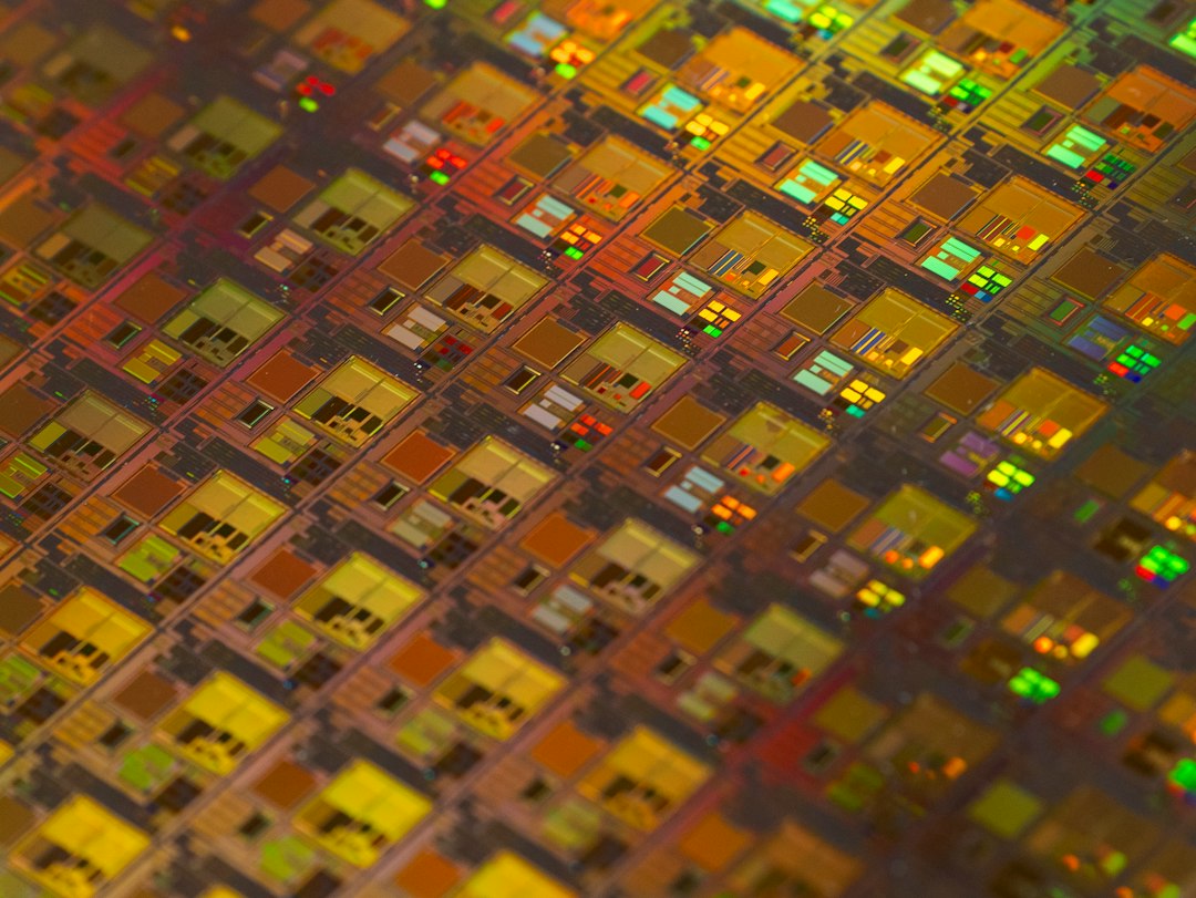
    a close up of a pattern of small squares
    Photo by Maxence Pira on Unsplash
    Key facts

    • Samsung Executive Chairman Lee Jae-yong visited the Advanced Package Lab (APL) in Yokohama, Japan, on Sunday, according to Hankyoreh and The Korea Times.
    • APL began operating in 2023 and held its official opening ceremony on September 8 this year, per Hankyoreh and Korea Times.
    • Samsung Electronics has been investing 40 billion yen (about $254 million) over five years starting in 2024 to build the lab's research infrastructure, according to Korea Times.
    • Lee was accompanied by Kawahira Hiroichi, vice president and head of DS Research Japan, and Kariya Takashi, the executive director leading APL, per Hankyoreh.
    • Last month, Lee reportedly called Samsung's chip division head Jeon Young-hyun and devices division head Roh Tae-moon to Japan for a related meeting, according to Hankyoreh.

    What happened

    Lee toured the Advanced Package Lab (APL), accompanied by Kawahira Hiroichi, vice president and head of DS Research Japan, and Kariya Takashi, the executive director who leads APL, Hankyoreh reported. During the visit, Lee checked on the development of materials and process technologies used in advanced semiconductor packaging and spoke with researchers about expanding ties with Japan’s materials, parts and equipment companies, according to the outlet. The Korea Times added that Lee pledged to keep growing APL’s research staff and to turn it into a global hub for next-generation packaging work.

    The trip followed an earlier gathering last month, when Lee reportedly summoned Samsung’s semiconductor division head Jeon Young-hyun and its devices division head Roh Tae-moon to Japan for discussions, Hankyoreh noted.

    Why it matters

    Advanced packaging involves combining different chip components — such as GPUs, high-bandwidth memory, and accelerator chips — into a single package. This step directly affects how an AI system performs in terms of data bandwidth, power efficiency, and heat management, according to Hankyoreh. As global demand for AI processors rises, packaging technology is increasingly seen as being just as important as chip fabrication itself.

    Lee reportedly stressed that securing strong packaging capabilities is critical, since these techniques are becoming central to competitiveness in AI processor chips, according to Korea Times.

    a large body of water with a city in the background
    Photo by bady abbas on Unsplash

    Background

    APL began operating in 2023 and held its formal opening ceremony on September 8 this year, according to both Hankyoreh and Korea Times. Samsung Electronics said it has been investing 40 billion yen, roughly $254 million, over five years starting in 2024 to build research infrastructure in Japan and strengthen its packaging technology, Korea Times reported.

    The lab is meant to connect Samsung’s chip design and manufacturing operations with Japan’s network of materials, parts, and equipment suppliers, including firms like Tokyo Electron and Ibiden, according to Hankyoreh. APL’s research focus differs from that of the packaging unit at Samsung’s Semiconductor R&D Center in Korea, and the two teams plan to coordinate closely for added synergy, Korea Times reported.

    Samsung also pointed to Japan’s government support for the semiconductor and AI sectors as a reason the country remains an attractive base for packaging research and local partnerships, according to a company statement cited by Hankyoreh. More broadly, Japan has long been home to a dense network of specialized chip equipment and materials makers, giving global chipmakers access to an established supply chain even as the country builds fewer leading-edge chip factories than some competitors.

    What to watch

    Future signals to track include whether APL expands its headcount and research scope as Samsung has indicated, and whether the company deepens its sourcing relationships with Japanese materials and equipment firms. Our read: the visit suggests Samsung sees packaging technology, not just transistor miniaturization, as a key front in the broader AI chip race, with Japan’s supplier base playing a growing part in that strategy. Additional announcements on investment levels, staffing, or specific technology milestones at APL would offer clearer evidence of how quickly this approach is advancing.

    Frequently asked questions

    What is Advanced Package Lab (APL)?

    APL is Samsung Electronics' semiconductor packaging research site in Yokohama, Japan, that develops and tests materials and process technologies for advanced chip packaging, according to Hankyoreh and Korea Times.

    How much has Samsung invested in the Japan lab?

    Samsung Electronics has been investing 40 billion yen, about $254 million, over five years starting in 2024 to build research infrastructure there, per Korea Times.

    Why does packaging matter for AI chips?

    Advanced packaging combines components like GPUs, high-bandwidth memory, and accelerator chips into a single unit, directly shaping an AI system's bandwidth, power efficiency, and heat performance, according to Hankyoreh.

    Sources

    This article was prepared with AI assistance from the reports listed above and automatically checked against them. See About for how we work.